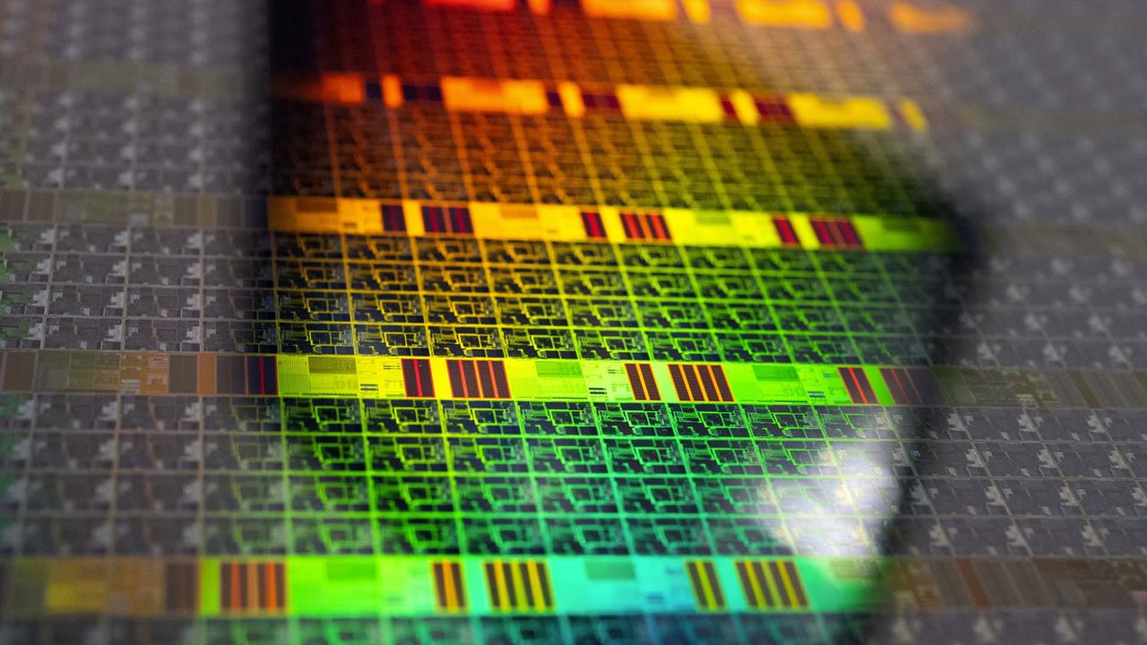
Revolutionary Transistor Stacking Technique Promises to Revitalize Moore’s Law
At Gaming News, we are at the forefront of groundbreaking technological advancements, and today we bring you an in-depth look at a development that promises to redefine the future of computing. Electronics researchers have unveiled a novel transistor stacking methodology that could very well be the key to extending the life of Moore’s Law for years to come. This breakthrough isn’t just an incremental improvement; it’s a paradigm shift in how we conceptualize and implement the fundamental building blocks of our digital world. Imagine the intricate dance of logic gates and memory cells, not spread out horizontally, but stacked vertically, creating unprecedented levels of density and efficiency. This is the essence of their ingenious design, a sophisticated evolution in semiconductor fabrication that could usher in a new era of accelerated technological progress.
The Impending Stagnation of Moore’s Law and the Quest for a Solution
For decades, Moore’s Law, the observation that the number of transistors on a microchip doubles approximately every two years, has been the guiding star of the semiconductor industry. This exponential growth has fueled the relentless march of innovation, leading to smaller, faster, and more powerful electronic devices. However, as transistors shrink to atomic scales, we are encountering fundamental physical limitations. The economic viability of scaling down further is becoming increasingly challenging, and the heat dissipation issues associated with densely packed transistors are reaching critical thresholds. These roadblocks have led many to believe that the era of Moore’s Law is drawing to a close, posing a significant threat to the continued advancement of computing power, artificial intelligence, and even the cutting-edge graphics demanded by the gaming world. The industry has been desperately searching for a way to circumvent these obstacles, exploring new materials, architectures, and manufacturing techniques. This new stacking approach represents a monumental leap forward in that search, offering a tangible path to sustained progress.
Understanding the Core Innovation: A Vertical Integration Approach
The core of this revolutionary development lies in its vertical integration of transistors. Unlike traditional planar fabrication where transistors are laid out side by side on a silicon wafer, this new method allows for the layering of multiple transistor structures directly on top of one another. This is akin to transforming a sprawling single-story factory into a multi-level skyscraper, dramatically increasing the usable space within a given footprint.
The “One Potato, Two Potato” Analogy: A Simpler Perspective
To grasp the essence of this breakthrough, consider the simple children’s counting rhyme, “One potato, two potato, three potato, four.” In traditional chip design, this would translate to laying out four distinct “potatoes” (transistors) side-by-side on a flat surface. The new method, however, allows us to stack these “potatoes” vertically. We can place one “potato” on top of another, then another, and so on, all within the same lateral space. This analogy, while elementary, perfectly captures the fundamental principle of achieving greater density without sacrificing lateral area. The implications for miniaturization and performance are profound. Instead of needing more land (chip area) to house more components, we are building upwards, maximizing the utility of the existing substrate.
Key Architectural Shifts: Beyond Planar Limits
This vertical stacking isn’t merely a cosmetic change; it necessitates a fundamental re-imagining of transistor architecture and interconnectivity. The researchers have devised ingenious ways to ensure that these vertically stacked transistors can communicate with each other efficiently and with minimal signal degradation. This involves developing new wiring schemes and inter-layer dielectric materials that can handle the increased complexity of three-dimensional connections. The challenges here are immense, requiring precise control over material deposition, etching, and lithography at scales previously thought impractical.
Technical Deep Dive: Unpacking the Stacking Methodology
Delving deeper into the technical specifics, the researchers have employed a series of advanced fabrication techniques to realize this vertical transistor architecture. This is not a simple “plug and play” solution; it requires meticulous engineering at every stage.
Advanced Lithography and Etching for Vertical Structures
The creation of these multi-layered transistor structures relies heavily on state-of-the-art lithography techniques. These techniques are capable of defining incredibly small features with extreme precision, a prerequisite for building such intricate vertical arrangements. Furthermore, anisotropic etching processes are crucial for carving out the precise channels and gate structures needed for each layer of transistors. The ability to etch deeply and selectively without damaging the underlying layers is paramount. The control required is extraordinary, ensuring that each transistor in the stack functions independently while still being part of a unified circuit.
Novel Interconnects and Via Technologies
One of the most significant hurdles in vertical integration is the management of electrical connections between layers. Traditional interconnects are designed for planar layouts. The researchers have developed new metallization schemes and advanced via technologies to bridge these vertical gaps. These vias, essentially tiny conductive pillars, must be perfectly aligned and conduct electricity with minimal resistance. The materials used for these interconnects are also critical, often involving low-resistance metals and specialized insulating layers to prevent short circuits. The efficiency of these interconnections directly impacts the overall performance and power consumption of the chip.
Materials Science Innovations: Enabling Layered Functionality
The success of this stacking method is also dependent on advances in materials science. The researchers are employing new semiconductor materials and dielectric layers that can withstand the high temperatures and pressures involved in the fabrication process, while also offering optimal electrical and thermal properties. The selection and integration of these materials are critical for ensuring the long-term reliability and performance of the stacked transistors. This includes exploring materials that can facilitate efficient heat dissipation, a persistent challenge in densely packed integrated circuits.
The Impact on Performance and Efficiency: A Leap Forward
The implications of this breakthrough for computing performance and energy efficiency are nothing short of transformative. By packing more transistors into the same area, we can achieve significant gains in processing power.
Accelerated Computational Speeds
With transistors stacked vertically, the physical distance data needs to travel between them is drastically reduced. This shorter path translates directly into faster switching speeds and consequently, higher computational speeds. Imagine complex calculations that used to take milliseconds now completing in microseconds. This acceleration is particularly crucial for demanding applications like high-fidelity gaming, real-time simulations, and complex AI model training. The ability to process information more quickly opens up new possibilities for what our devices can achieve.
Enhanced Power Efficiency and Reduced Heat Generation
While it might seem counterintuitive, vertical stacking can also lead to improved power efficiency. Shorter interconnects mean less energy is lost as heat during data transmission. Furthermore, the ability to integrate more functionality into a smaller footprint can allow for the design of more power-efficient chip architectures. This is a double win: faster performance and lower power consumption, which translates to longer battery life for mobile devices and reduced energy costs for data centers. The challenge of heat dissipation remains, but the new architectural approaches are designed with thermal management as a central consideration.
Unlocking New Levels of Miniaturization
This innovative stacking technique offers a compelling solution to the physical limitations that have been hampering further miniaturization. By building in three dimensions, we can continue to shrink the overall size of our electronic devices without compromising on their capabilities. This opens doors for entirely new form factors and applications, from ultra-compact wearable technology to highly integrated systems for advanced robotics. The potential for embedding more computing power into everyday objects is immense.
Applications Across Industries: Beyond the Gaming Realm
While the gaming industry stands to benefit immensely from this advancement, the applications of this revolutionary transistor stacking extend far beyond.
The Future of High-Performance Gaming and Graphics
For gamers, this breakthrough translates directly into more immersive and visually stunning experiences. We can anticipate next-generation gaming consoles and PC components capable of rendering incredibly detailed worlds, supporting complex physics simulations, and achieving higher frame rates with unprecedented smoothness. The ability to pack more powerful graphics processing units (GPUs) into smaller form factors will also pave the way for portable gaming devices with desktop-class performance. This is a game changer for the entire gaming ecosystem.
Accelerating Artificial Intelligence and Machine Learning
The insatiable demand for computational power in artificial intelligence (AI) and machine learning (ML) is a perfect match for this new stacking technology. Training complex neural networks requires massive parallel processing capabilities. This vertical integration allows for the creation of more compact and powerful AI accelerators, enabling faster model training, more sophisticated AI algorithms, and the deployment of advanced AI in a wider range of applications, from autonomous vehicles to personalized medicine.
Advancements in High-Performance Computing (HPC) and Data Centers
High-performance computing (HPC) environments and data centers are constantly seeking ways to increase processing density and reduce power consumption. This new stacking method offers a significant advantage by allowing for more powerful servers in smaller footprints, leading to reduced infrastructure costs and energy footprints. The ability to perform complex simulations and data analysis at unprecedented speeds will accelerate scientific discovery and drive innovation across numerous fields.
Transforming Mobile Devices and Wearable Technology
The drive for thinner, lighter, and more powerful smartphones, tablets, and wearables will be significantly boosted by this technology. Imagine devices with the processing power of today’s high-end laptops fitting comfortably into your palm, or smartwatches capable of running advanced applications without compromising battery life. This unlocks new possibilities for personal computing and connectivity on the go.
Challenges and the Road Ahead: Navigating the Transition
While the potential is enormous, the path from laboratory breakthrough to widespread commercial adoption is not without its challenges.
Manufacturing Scalability and Yield Rates
The primary challenge lies in scaling up the manufacturing process. The intricate nature of vertical stacking requires highly precise and complex fabrication steps. Achieving consistently high yield rates (the percentage of functional chips produced) at these scales will be critical for economic viability. This will require significant investment in new manufacturing equipment and refined production methodologies.
Economic Viability and Cost of Production
The cost of producing these vertically stacked chips will be a crucial factor in their market penetration. While the long-term benefits in terms of performance and efficiency are clear, the initial manufacturing costs may be higher than traditional planar chips. Overcoming this will require continued innovation in materials and processes to drive down production expenses.
Testing and Reliability in Three Dimensions
Ensuring the long-term reliability and robust performance of these three-dimensional transistor structures presents unique testing challenges. The complex interconnections and layered architecture require new testing methodologies to identify and mitigate potential failure points. Rigorous validation will be essential to build confidence in the technology.
Conclusion: A New Horizon for Computing Power
The development of this revolutionary transistor stacking technique marks a pivotal moment in the evolution of computing. It offers a powerful and viable path to sustain the spirit of Moore’s Law, ensuring that our electronic devices continue to become more powerful, efficient, and capable. At Gaming News, we are thrilled to witness these advancements, which promise to unlock unprecedented levels of performance for gaming and beyond. This breakthrough is not just about more transistors; it’s about a smarter, more efficient, and more powerful way to build the digital infrastructure of our future. The era of truly three-dimensional integrated circuits is dawning, and it promises to redefine what’s possible in the world of technology.